

An SRAM is composed of rows and columns forming a matrix of memory cells. The rows are known as Word Lines (WL) and control the access to the cells of that line, defining when it's possible to get or change the stored data. On the other hand, the columns are known as Bit Lines (BL), Digit Lines or Data Lines, and are responsible to conduct the data to and from the cells, either in a write or read operation, respectively. Bit Lines generally exist in pairs, opposite to each other (BL and ~BL). Finally, there are the memory cells, small circuits which are able to store 1 bit.
This image represents the basic structure of an SRAM memory:

Let's analyse the cell itself. The cell is able to store 1 bit, and its internal structure is composed of 6 transistors, where 4 of these, form 2 crossed inverters: Q1, Q2, Q3, Q4, which are responsible for keeping the data stored, as long as the memory is powered. The other 2 transistors, Q5 and Q6 serve as gateways for bidirectional access between stored data and the Bit Lines. These access transistors are controlled with the Word Line.
The following diagram represents a typical 6T memory cell:


When φS is equal to '1', the higher voltage line will define the state of the inverters, and consequently assign the correct logic levels to the respective Bit Lines. When φS is equal to '0', the amplifier is turned off. There will be a Sense Amplifier for each of the columns in the memory.
Each column is also equipped with a Pre-charge and Equalizing circuit:

Combining all the previous circuits together, we get the column internal structure:

First, the reading operation:

Now the writing operation, considering we want to write '0' and that '1' is stored:

Now that the diagrams and functioning of the cell are comprehended we can move on to the semiconductor layout. In the following layouts I've used the rules of CMOS 0.18 μm technology.
Here is the layout of the SRAM cell itself:
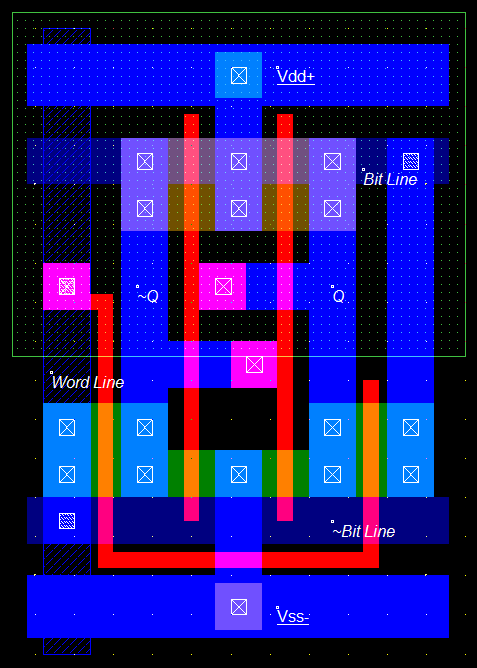
The cell layout has the following size:
Width: 5.8μm (56 lambda)
Height: 8.0μm (80 lambda)
Surface: 46.4μm2 (0.0 mm2)
Now the Sense Amplifier layout:

These are the Sense Amplifier specifications I've obtained:
Width: 7.8 μm (78 lambda)
Height: 7.8 μm (78 lambda)
Surface: 60.8 μm2 (0.0 mm2)
Finally the Pre-charge and Equalizing circuit layout:

These are the Pre-charge and Equalizing transistors specifications:
Width: 3.0 μm (30 lambda)
Height: 7.6 μm (76 lambda)
Surface: 22.8 μm2 (0.0 mm2)
Now we can unite all the previous elements: the cell, the sense amplifier and the pre-charge and equalizing circuit, and put together an SRAM memory of 1x1 bit:
These are the properties of this layout:
Width: 24.9μm (249 lambda)
Height: 8.6μm (86 lambda)
Surface: 214.1μm2 (0.0 mm2)
*NOTE: On this layout the column is represented horizontally and the lines vertically, only for practicality reasons during its design.
With the 1x1 bit SRAM finished it's time to move on to the simulation. For this let's consider we want to save the the logic level '1' in the memory, then we will perform a reading operation. After this, I'll store the value '0' and read the memory once again.
These are the necessary proceedings to write on the memory cell:
- Turn off the Sense Amplifier (φS = 0) and activate the Pre-charge and Equalizing circuit momentarily (φP = 1).
- Shut down the Pre-charge circuit (φP = 0), prepare the data to be written (Data In = 1) and give the write instruction (WE = 1).
- Activate the Sense Amplifier (φS = 1) to amplify the logic levels on the Bit Lines.
- Activate the Word Line (WL = 1) to turn on the gateway transistors, connecting the Bit Lines with the cell, allowing its value to be changed.
- Turn off the Sense Amplifier (φS = 0) and activate the Pre-charge and Equalizing circuit momentarily (φP = 1).
- Shut down the Pre-charge circuit (φP = 0).
- Activate the Word Line (WL = 1) to turn on the gateway transistors, connecting the Bit Lines with the cell. The stored data will propagate to the Bit Lines.
- Activate the Sense Amplifier (φS = 1) to amplify the logic levels on the Bit Lines and give the read instruction (RE = 1).
These are the results of the first 1 bit SRAM simulation:
The following diagram is the result of that Winspice simulation:
As we can observe on both simulations, the first action is the activation of the Pre-Charge circuit when t = 1 ns, which immediately changes the voltage on both Bit Lines, stabilizing them around VDD/2. Then, when t = 2 ns, the logic level '1' is preloaded onto the Data In input, while at the same time is given the write instruction and the Sense Amplifier is turned on. This affects the Bit Lines, where in BL the voltage rises towards VDD and in ~BL decreases towards VSS. After a little instant, the word line is activated when t = 3 ns, which makes the voltage in Q rise up to VDD, changing the logic level to '1' on the memory cell, while the opposite occurs in ~Q. After this, the word line is deactivated, together with the Sense Amplifier and the write instruction. At this point, it no longer matters what signal is placed on the Data In input, because as we can see, the memory cell already memorized the value '1' in Q. This is also true for the Bit Line, however, the voltage only remains the same in here because of the parasitic capacity of the Bit Lines.
At 6 ns begins the reading operation of the cell, the Pre-Charged is activated again, stabilizing the Bit Lines around VDD/2. At 7 ns the word line is turned on, allowing the stored values on the cell to propagate onto the Bit Lines, overcoming the residual voltages they have left, while the Sense Amplifier is also activated and the read instruction is given, which makes the values reach the Data Out terminal. When t = 8 ns the word line is turned off, together with the Sense Amplifier and the reading instruction, while the stored value will keep itself on the Bit Line and Data Out terminal, again because of their parasite capacities.
It should be noted that, although the desired value to be read should be VDD, the Data Out terminal presents a slightly smaller value, which doesn't happen on the Bit Line, this occurs because of the Body Effect. Since the read/write selector was made only with NMOS transistors, there is no symmetry on this part of the circuit, so instead of VDD, the output will be VDD-VT.
From the 10 ns mark the process repeats itself, where in this time it will be stored the logic level '0' onto the memory cell.
Now let's finally focus on the real objective of this work, the 32 bit SRAM memory cell:
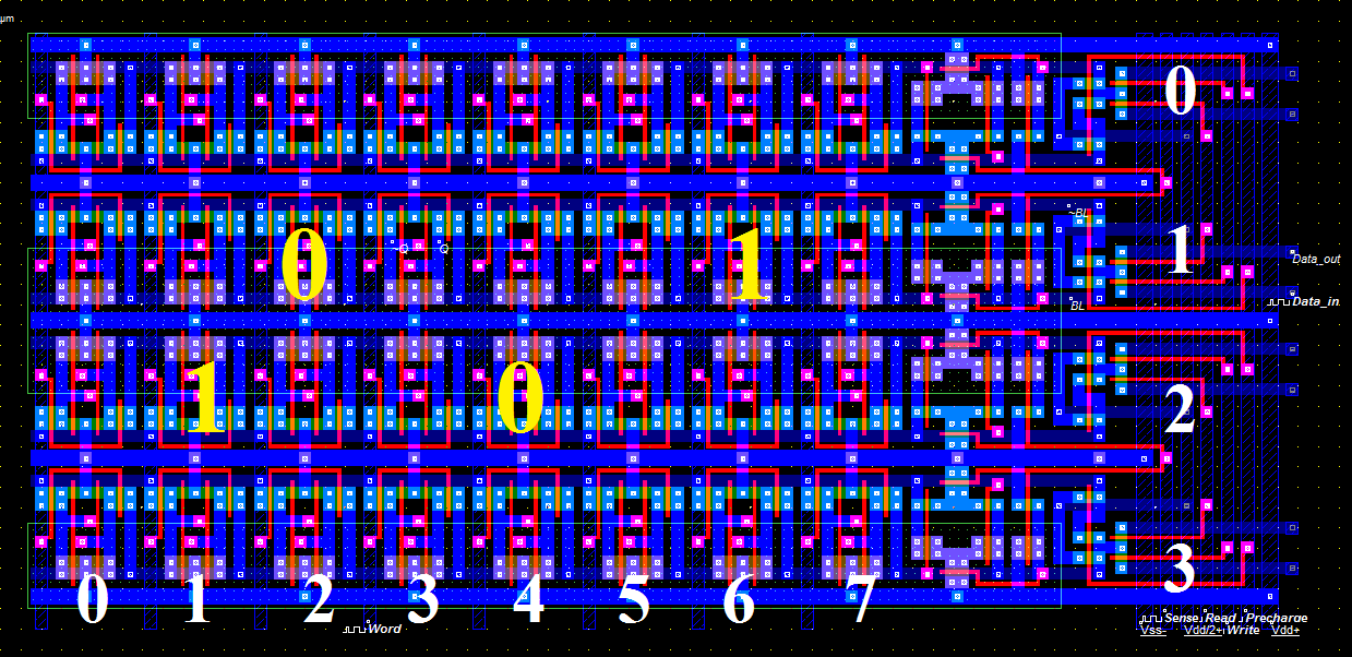
These are the properties of the layout:
Width: 62.7 μm (627 lambda)
Height: 29.4μm (294 lambda)
Surface: 1843.4μm2 (0.0 mm2)
Moving on to the 32 bit SRAM simulation, let's consider we want to write the data in the respective positions, indicated by the previous image (in yellow). In summary I'll attempt to write:
- '1' - On column 2, row 1 - Q[2,1]
- '0' - On column 1, row 2 - Q[1,2]
- '0' - On column 2, row 4 - Q[2,4]
- '1' - On column 1, row 6 - Q[1,6]

This is the result of the 32 bit SRAM simulation:

The correct values are stored in the desired positions. The first '1' is stored in Q[2,1] at 3 ns, then '0' at Q[1,2] around 8 ns, although it is unnoticeable on the diagram, since the previous value was also zero. The same happens for the '0' in Q[2,4] at 13 ns. Then the final '1' is stored in Q[1,6] at 18 ns.
For the reading operation we can observe at 22 ns the value of Q[2,1] being transferred to DOUT[2] and then Q[1,2] to DOUT[1] at 26 ns, again difficult to see because of the same previous value, also happening for Q[2,4] and DOUT[2] at 30 ns. Finally, the last reading takes place at 34 ns when the value '1' is copied from Q[1,6] to DOUT[1].
By analysing this diagram we can conclude that the memory is working properly.
And this is it. Overall this has been quite an interesting work since it has allowed me to understand how digital memories work, how they are designed, what basic elements and circuits are necessary, and how these elements can be put together to achieve a functional memory.
I've also made the SRAM 1x1 bit Winspice simulation file (.cir) available here.
Excellent explanation. Very complete. Good job.
ReplyDeleteCan you explain those 2 transistor part which you did for cenencting bitlines with data in or data out terminals.
ReplyDeleteThat's just for simulation purposes. Usually a finished memory design has line and column decoders and also I/O buffers. Since I needed to connect the Bit lines to the data in or data out lines, according to the respective simulation procedure, write/read cycle. So basically it's simply a switch, where the controller is the read/write inputs.
DeleteHow did you use read/write and dataIn/DataOut in your circuitry. I read your previous comment where you mentioned them as a switch but can you please show us that part as well. I am trying to design SRAM but got stuck in that part, so I am referring to your work as a starting point. You can reply me in my email:
ReplyDeletewqer1988@gmail.com
Best regards
Waseem Qader
Well it's basically just following the procedures I described. As I explained above, 4 steps for the write cycle and 4 steps for the read cycle. If you're asking about how to actually do it for yourself, well I guess it will depend on the program you're using, usually you can assign properties to each terminal/label such as a clock, a pulse or a PWL, which allows you to create a table and define your own function in time and voltage.
Deletehow i design 8t sram sense amplifier??
ReplyDeleteHow does precharge and equalizer circuit work to charge the bitlines to Vss/2?
ReplyDeleteThrough transistors Q8 and Q9.
DeleteWhere are column and Row decoder in circuit?
ReplyDeleteSend me all ckts with waveforms and output
ReplyDelete